
With the support of BWT femtosecond laser, Tianjin University's breakthrough in photoacoustic remote sensing microscopy technology reaches new heights!
Recently, Professor Tian Zhen's team at Tianjin University achieved a significant breakthrough in the field of photoacoustic remote sensing microscopy technology, successfully developing a new non-destructive testing method. This technology utilizes BWT's high-power femtosecond laser as the key light source, further optimizing the solution to the internal flaw detection limitation problem in inverted chip. It enhances the overall detection performance of the system, opening a new chapter in the development of non-destructive testing technology.

1. Taking the Lead, Boosting the Leap of Non-Destructive Testing Technology
Photoacoustic remote sensing microscopy technology, proposed in recent years as a promising microscopic detection method, enables large field-of-view, rapid, non-destructive imaging of internal structures in inverted chip models, which is of great significance for the detection of high-value objects such as chips and biological tissues.
Researchers explained that traditional microscopy techniques often face the dilemma of either limited imaging depth or resolution. Either the imaging depth is insufficient, such as in OCT, or the resolution is not high, and there is contact involved. Photoacoustic remote sensing microscopy technology can significantly address these pain points, achieving characteristics such as large imaging depth, high resolution, and non-contact imaging. It holds high value in medical applications.
In the study, Tianjin University utilized BWT's 20-watt infrared femtosecond laser as the femtosecond laser source, providing stable and high-quality laser pulses for photoacoustic remote sensing microscopy. The laser outputs with a central wavelength of 1030 nm, an adjustable repetition rate of 0.1-1 MHz, and an adjustable pulse width of 300 fs-10 ps (the pulse width used in the experiment is approximately 1.2 ps).
After collimation and beam expansion, the laser pulse was combined with the continuous probing light emitted by a super-radiating light-emitting diode with a wavelength of 1310 nm. It then entered the optical scanning system, consisting of a scanning mirror system, an objective lens, and a three-dimensional electric displacement stage, for large field-of-view rapid scanning imaging. During imaging, the inverted chip is in an inverted state, where the internal metal structure is not visible under bright-field microscopy, as shown in Figure 1 (b).
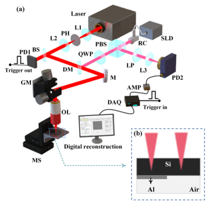
Figure 1: Schematic diagram of photoacoustic remote sensing system
for non-destructive inspection of inverted chips.
The photoacoustic remote sensing microscopy system can perform large field-of-view optical-mechanical joint scanning imaging of inverted chip models. Its working principle is to first obtain independent small field-of-view images through "mosaic scanning", then use the electric displacement stage to move the chip sample to the next adjacent position, and finally stitch these small range images to form a complete large field-of-view image, as shown in Figure 2. The experimental results fully demonstrate the potential of photoacoustic remote sensing microscopy for non-destructive testing of chips in industrial environments.
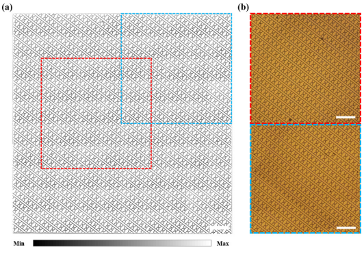
Figure 2: Optical scanning imaging results (scale: 300 μm).
The successful application of this technology will significantly improve the overall detection performance of the system and is expected to become an important tool for non-destructive testing in the medical field, providing strong support for the early detection and precise treatment of diseases.
2. Femtosecond Laser: A Powerful Engine for Scientific Innovation
BWT's high-power femtosecond laser, with outstanding stability, adjustable pulse width, and good beam quality, provides strong support for scientific research fields such as photoacoustic remote sensing microscopy technology.
This 20-watt infrared femtosecond laser, benefiting from its all-fiber structure and industrial integration design, demonstrates excellent stability and processing capabilities. Its features include long-term continuous processing stability, adjustable pulse width, repetition rate, and adjustable pulse energy, enabling pulse time-domain control within 300 femtoseconds, effectively reducing the thermal impact on material processing and achieving true "cold" processing.
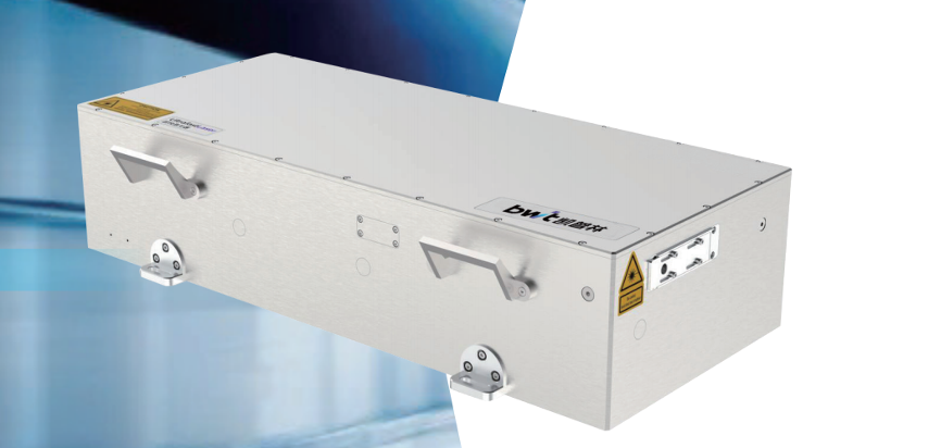
Bwt's 20-watt Infrared Femtosecond Laser
This laser is widely favored in the field of organic film and flexible material processing, and it has also attracted much attention in the domestic ultrafast laser market. It can not only handle flexible and fragile materials such as OLED, glass, ceramics, sapphire, diode materials, and alloy metals, but also plays an important role in micro-nano processing, precision marking, and other precision processing applications.
In the realm of ultrafast lasers, small-scale precision is where they shine. The head of BWT's ultrafast laser division stated that ultrafast lasers have enormous development potential, continuously expanding the boundaries of human cognition in frontier fields and continuously overcoming key technological challenges in application areas. Looking ahead, BWT will adhere to a long-term vision, delve deeper into femtosecond, picosecond, and nanosecond laser fields, provide more innovative solutions for scientific research and industrial applications, and promote the progress and development of technology.